A bipolar junction transistor (BJT) is a type of transistor. It is a three-terminal device constructed of doped semiconductor material and may be used in amplifying or switching applications. Bipolar transistors are so named because their operation involves both electrons and holes.
Although a small part of the transistor current is due to the flow of majority carriers, most of the transistor current is due to the flow of minority carriers and so BJTs are classified as 'minority-carrier' devices.
- the emitter–base junction is forward biased
- the base–collector junction is reverse biased
- the equilibrium between thermally generated carriers and the repelling electric field of the depletion region becomes unbalanced
- allowing thermally excited electrons to inject into the base region
- These electrons wander (or "diffuse") through the base from the region of high concentration near the emitter towards the region of low concentration near the collector
- The electrons in the base are called minority carriers because the base is doped p-type which would make holes the majority carrier in the base.
.svg.png)
The base region of the transistor must be made thin, so that carriers can diffuse across it in much less time than the semiconductor's minority carrier lifetime, to minimize the percentage of carriers that recombine before reaching the collector–base junction. To ensure this
- the thickness of the base is much less than the diffusion length of the electrons
- the emitter region
- the base region
- the collector region

- emitter (E)
- base (B)
- collector (C)


In the diagram, the arrows representing current point in the direction of the electric or conventional current—the flow of electrons is in the opposite direction of the arrows since electrons carry negative electric charge. The ratio of the collector current to the base current is called the DC current gain. This gain is usually quite large and is often 100 or more.
 Narrowing of the base width has two consequences:
 - There is a lesser chance for recombination within the "smaller" base region.
- The charge gradient is increased across the base, and consequently, the current of minority carriers injected across the emitter junction increases.
Both factors increase the collector or "output" current of the transistor in response to an increase in the collector–base voltage.
In the forward active region the Early effect modifies the collector current (iC) and the forward common emitter current gain (βF) as given by the following equations:[citation needed]
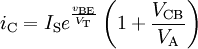

Where
-
- VCB is the collector–base voltage
- VA is the Early voltage (15 V to 150 V)
- βF0 is forward common-emitter current gain when VCB = 0 V


1 comment:
tlg aq.alang2 ko dah stdy p-n junction,nnt leh tlg kaitkan p-n junction dlm solar cell..tlg lorr aq yg terkapai2 ni
Post a Comment